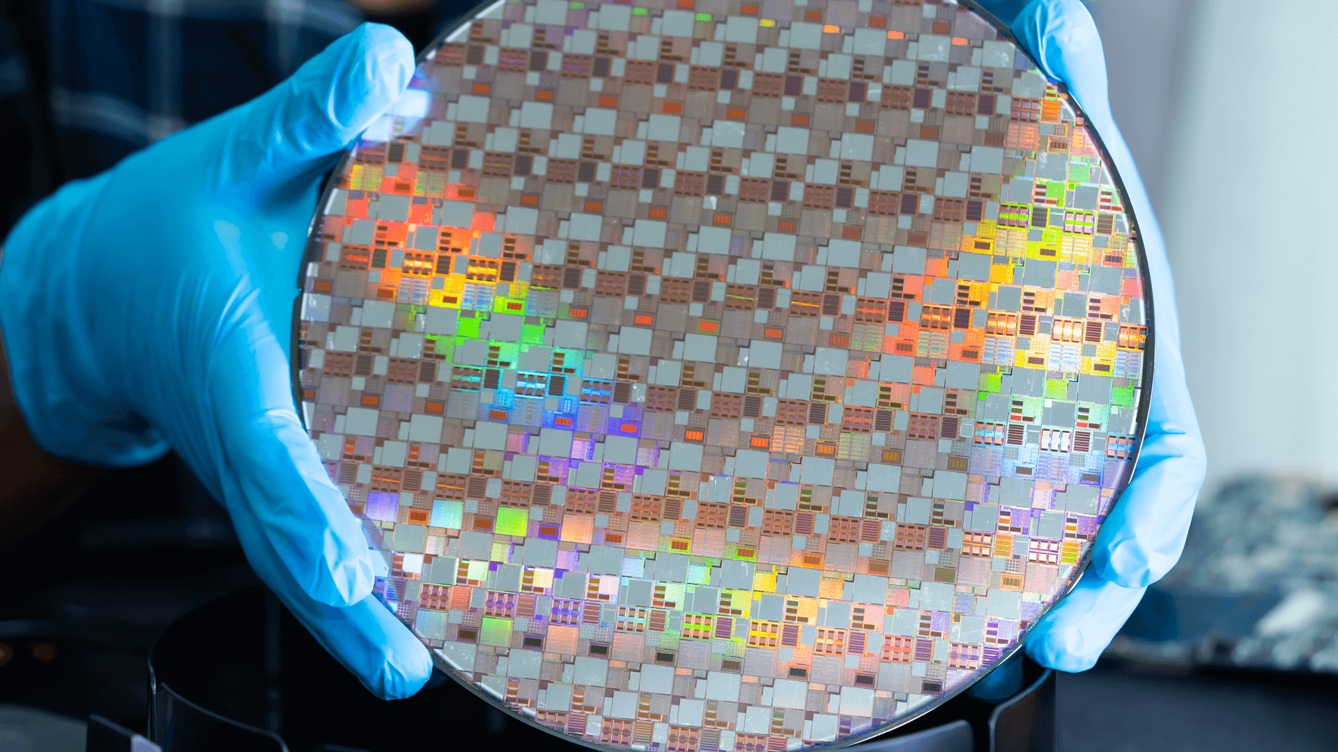
Power semiconductor devices are key enablers for the whole power electronics industry. e.g., for electric mobility and renewable energy solutions. This industry is expected to massively grow to $26 billion in 2026. Major reason for the shift is the requirements of the European Green Deal. Meaning, transformation the EU into a fair and prosperous society with a modern and competitive economy.
Massive challenges that AddMorePower will overtake is to better manage the rapid and massive spread of the power electronics.
More precisely AddMorePower aims to advance X-ray and electron-probe related characterization techniques as well as modelling approaches for new wide bandgap power semiconductor materials, 3D integrated power technologies and the correlated modelling workflows. The wide impact of AddMorePower will broaden and accelerate market penetration, promote material integration and development for European power semiconductor technologies and provide new opportunities for other mono- and polycrystalline based industries.

About
Vision
At AddMorePower we see the opportunity to advance power semiconductor technology and increase the share of wide bandgap power devices supplied by European manufacturers as a main vision of the project. AddMorePower aims to refine FAIR data-management methods to enhance and efficiently use characterization data (using CHADA).
We are aware that in order to better develop processes on significantly larger market scale, semiconductor manufacturers urgently need to find better ways of efficiently analysing and classifying lattice defects as well as the degradation dynamics of Cu power metallization.
This is where AddMorePower will step in to help fill-in the gap, master the development and integration of the new technology and accumulate know-how for the further use and application in various industries.
Keyfacts
Reference
Reference Number:
101091621
Programme type:
Horizon Europe
Programme acronym:
HORIZON-CL4-2022-RESILIENCE-01-19
Duration
Project Start:
01.01.2023
48 Months
Cost and Funding
Costs: € 5.995.526,25
Funding:
100,00% EU-funded
Motivation
Power semiconductor devices are key enablers for the whole power electronics industry. This industry is expected to massively grow to $26 billion in 2026. Major reason for the shift is the requirements of the European Green Deal. Europe’s future depends on a healthy planet.
Meaning, EU countries are committed to achieving the ultimate goal of climate neutrality by 2050. Aligned with the new EU strategy, AddMorePower aims to add to the transformation of the EU into a fair and prosperous society with a modern and competitive economy.
Meaning, EU countries are committed to achieving the ultimate goal of climate neutrality by 2050. Aligned with the new EU strategy, AddMorePower aims to add to the transformation of the EU into a fair and prosperous society with a modern and competitive economy.
Mission and Objectives
AddMorePower’s mission is to overcome the limitations currently present in the power GaN, SiC, and related Cu metallization technologies, increase EU shares in power semiconductor production and enabling a more resilient European power electronics industry that will provide a solution to the emerging area of semiconductors.
The AddMorePower team will focus on the following objectives:
- Novel X-ray and electron-probe based characterisation workflows and protocols for power semiconductor materials
- Modelling concepts for better characterization and lifetime prediction of power semiconductor interconnect materials
- Establish FAIR and open data practices to enable efficient data workflows between characterization and modelling techniques
Work Packages
WP1
Project, risk and innovation management
01.01.2023
31.12.2026
Detailed information
Aligned for operational management and technical vitality. With the main objective to respond to opportunities through active research and innovation management.
WP2
Data management and workflows
01.01.2023
31.12.2026
Detailed information
Laying the ground for open science practices to enable open knowledge transfer between (industrial) research facilities and implementation of a FAIR data.
WP3
Advanced X-ray-based characterization methods
01.01.2023
31.12.2026
Detailed information
Develop advanced X-ray-based characterization methods to characterise morphological and structural properties of semiconductor substrates and nano-electronic devices, with high spatial resolution.
WP4
Advanced electron-based characterization methods
01.03.2023
31.12.2026
Detailed information
Develop techniques for microstructural and electrical characterization of dislocations in active semiconductor layers, identify critical types and provide a methodology and software package related to it.
WP5
Microstructure dependent multiscale and multiphysics modelling
01.01.2023
30.06.2026
Detailed information
Development and implement advanced models ranging from the scale of individual defects to single transistor cells including metallisation, addressing industrial needs by systematic mechanism-based upscaling models and describing individual defects and dislocations.
WP6
Demonstration and validation
01.01.2023
31.12.2026
Detailed information
Demonstrating and validating newly developed characterization and modelling techniques and aligning the characterization and modelling work packages so that industry-relevant problems can adequately be resolved.
WP7

Dissemination, communication, exploitation and standardisation
01.01.2023
31.12.2026
Detailed information
The main objectives are the targeted dissemination of the project and its results, internal and external communication of the project, contribution to the European Research Union, as well as the exploitation of the scientific results to create competitive advantage with innovative research and results.